Often it feels as if soldering is deemed to be more of an art form than something that’s underpinned by the cold, hard reality of physics and chemistry. From organic chemistry with rosin, to the material properties of fragile gold bond wires and silicon dies inside IC packages and the effects of thermal stress on the different parts of an IC package, it’s a complicated topic that deserves a lot more attention than it usually gets.
A casual inquiry around one’s friends, acquaintances, colleagues and perfect strangers on the internet usually reveals the same pattern: people have picked up a soldering iron at some point, and either figured out what seemed to work through trial and error, or learned from someone else who has learned what seemed to work through trial and error. Can we say something scientific about soldering?
Defining the problems
The problems that affect the soldering of components – whether it involves soldering by hand or reflow/wave-soldering – essentially come down to oxidation, moisture ingress and temperature cycling. The first one is fairly obvious: copper oxidizes, which means that solder will not make a good connection. The second is mostly related to the (plastic) packaging of components as they absorb moisture and the issues this can cause.
The third and last problem is by the far the most common thing which people argue about. Here the argument essentially concerns what constitutes a good solder joint. Often the use of a higher soldering temperature is listed as a good thing, as it supposedly shortens the soldering time per pad and with it the heating of the component, while also producing a better joint. In a moment we’ll see why that is not the case.
Moisture and soldering don’t mix
The moisture issue is something which one likely first encounters when ordering components from a store like Mouser or DigiKey and one receives the component in a bag that lists on the outside until what date the component can be soldered, along with a small card inside that has moisture-sensitive dyes on it to indicate whether moisture has entered the bag while it was in storage.
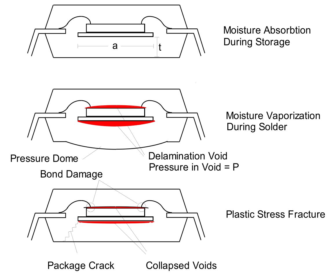
While at first this may seem strange, it begins to make sense when one realizes that the IC packaging isn’t water-proof, but that its molding compound will allow moisture through over time. While soldered into an active circuit, this isn’t a massive concern because it never gets hot enough to turn quickly into steam, but when soldering a component to the PCB, having moisture ingress can be fatal. The most extreme example of this is called ‘popcorning’. This concerns the heating up during soldering of moisture that has entered the molding component around the die:
As a result of this heating the moisture enters into a gaseous state, which massively increases its volume and consequently the pressure it exerts on the surrounding structures. This can crack the plastic molding, destroy features of the chip itself, break bond wires and so on. Essentially it will destroy the chip or damage it to the point where subsequent failure is unavoidable. A possible way to prevent damage from moisture ingress is by ‘baking’ the chip, gently heating the chip so that moisture is driven out of the chip packaging.
Soldering is an oxygen-free process
The main functions of solder flux are to remove existing oxidation, and to prevent new oxidation from forming. To accomplish the former, most flux contains one or more chemicals which begin to decompose when exposed to the heat from the soldering process, resulting in the formation of acids that will react with any oxidation on the surface to be soldered. Flux intended to be used with electronics will use weak acids, whereas the type used for pipe fitting will have significantly more aggressive acids, often using zinc chloride or other chlorides, which produce hydrochloric acid. Most often electronic flux will be rosin flux, also called resin flux.
Defining rosin is hard, as there are many forms and classifications. Important to note there is that the rough classification involves the natural rosin that is extracted from pine trees, natural rosin that has been chemically modified to be more heat-resistant, and synthetic rosin, usually called ‘resin’. Natural rosin is highly versatile, also finding uses in things like increasing the resistance of violin bow strings to make playing that instrument much easier.
Natural rosin flux is mildly active, but can be made stronger by adding different activator chemicals. This means that any type of rosin flux will have different properties, including a different activation and maximum temperature.
With the surface to be soldered on cleaned of oxidation, the acid has done its job. Next is to ensure that the surface doesn’t reoxidize while the component is being soldered down. This is done with chemicals whose task is to provide an oxygen barrier so that oxidation becomes impossible. Generally this is also the task of the rosin or equivalent substance. This means that the protective effect lasts for as long as this barrier is present. This property leads to the issue of soldering temperature.
Temperature: when more isn’t better
Because the conversion of rosin to acid depends on thermal activation, acid will be produced faster when the soldering temperature is increased. But this also means that the rosin gets used up faster and the oxygen barrier vanishes sooner. Higher temperatures also increase the oxidation rate, so there’s an optimal soldering window that is determined by both the amount of starting flux and the soldering temperature.
If we look at a common lead-based solder such as 245 CORE Sn63Pb37 from Kester, we can see from its Material Safety Data Sheet (MSDS) using the CAS number given for the rosin core (#65997-06-0) that it uses a modified rosin type from Eastman Chemical Company, called Staybelite Resin-E Partially Hydrogenated Resin. Its datasheet lists its properties as having a melting point between 55.2 °C and 72.1 °C, and a boiling point of 265 °C.
The recommended hand soldering temperature according to ESA (ECSS-Q-ST-70-08, section 5.6.7) is about 280-350 °C (up to 320 °C in the older PSS-01-708 standard), which in the case of the above lead-based solder means that the rosin flux will begin to activate first, at 55 °C, followed by the melting of the lead at about 184 °C (191 °C for 60/40 leaded). This gives about a 100-170 °C thermal window.
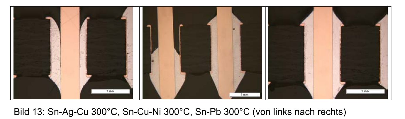
Research by Fraunhofer ISIT engineer Thomas Ahrens (link to PDF in German) examines what happens during various hand soldering temperatures. This research shows how higher soldering tip temperatures (300-375 °C) strongly reduces the time before PCB damage (‘measling’) occurs. It also shows for through-hole components that 300 °C produces excellent results, whereas the lead-free solders used (Sn-Ag-Cu, Sn-Cu-Ni) need a bit higher temperature to flow properly onto THT headers.
Don’t cycle that temperature
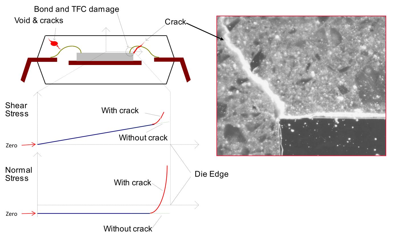
Along with the issue of moisture ingress – as covered earlier – IC packages are quite fragile structures, as is detailed exquisitely by Dr. Shirley at Portland State University in his presentation titled ‘Plastic Package Reliability‘. In addition to the moisture related issues, this document also covers heat-stress. Much of this is caused by thermal cycling during assembly, which can take a wide variety of shapes.
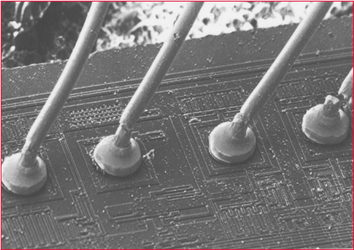
The effect of temperature cycling can cause new defects (e.g. cracks) in the molding compound, the die, bond wires and so on. It can also cause new cracks to be formed. This is why the ESA soldering standard referenced earlier requires that one attaches small heatsinks to the leads of any thermally sensitive devices. The effects of thermal cycling can be as disastrous as mechanical shearing literally destroying bond wires.
One may remember that in the datasheets for ICs one can usually find recommended and maximum soldering temperatures. These indicate just how warm the package can become before damage becomes inevitable. Since reality isn’t perfect, it’s a good idea to stay far below these indicated numbers in so far as possible. Even when damage isn’t immediately apparent, the action of over-heating part of an IC as well as heating it up and then cooling it down too quickly may have caused damage that may mean that the part will fail in a matter of weeks or months after assembly.
Putting it all together
The important message when it comes to soldering and doing it properly is that it’s all about the science behind it. At institutions like NASA, ESA, and those who make equipment for them, failure literally isn’t an option, which is why they have spent so much effort on understanding these failure modes and how to prevent them. Meanwhile manufacturers of solder and fluxes have many decades of knowledge and experience.
What is the price of doing things wrong? In hobby use, you can get away with pretty bad things when it comes to soldering. Chips won’t instantly die when soldered at 450 °C for two seconds without preheating, but one may have caused small fractures that will slowly destroy the chip during thermal cycles. If you use the gadget indoors for only a few years, you might never notice.
The important thing to know is what is needed to get that proper solder joint and not exceed it. When the science
shows that soldering lead-based at 300 °C works, then there’s no point in soldering at 375 °C. If anything, one risks poor joints by cooking off the rosin flux and getting oxidation on the pad before solder can bond with it.
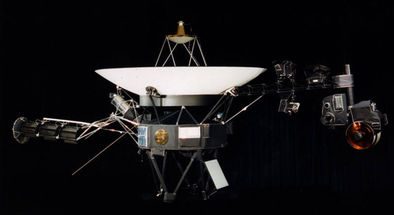
Finally, with NASA’s soldering practices they have had Spirit and Opportunity as well as many other Mars rovers and satellites perform flawlessly for years. Not to mention Voyager 1 and 2, traveling into interstellar space since they were launched in 1977. If those aren’t perfect solder joints, then I don’t know what are.