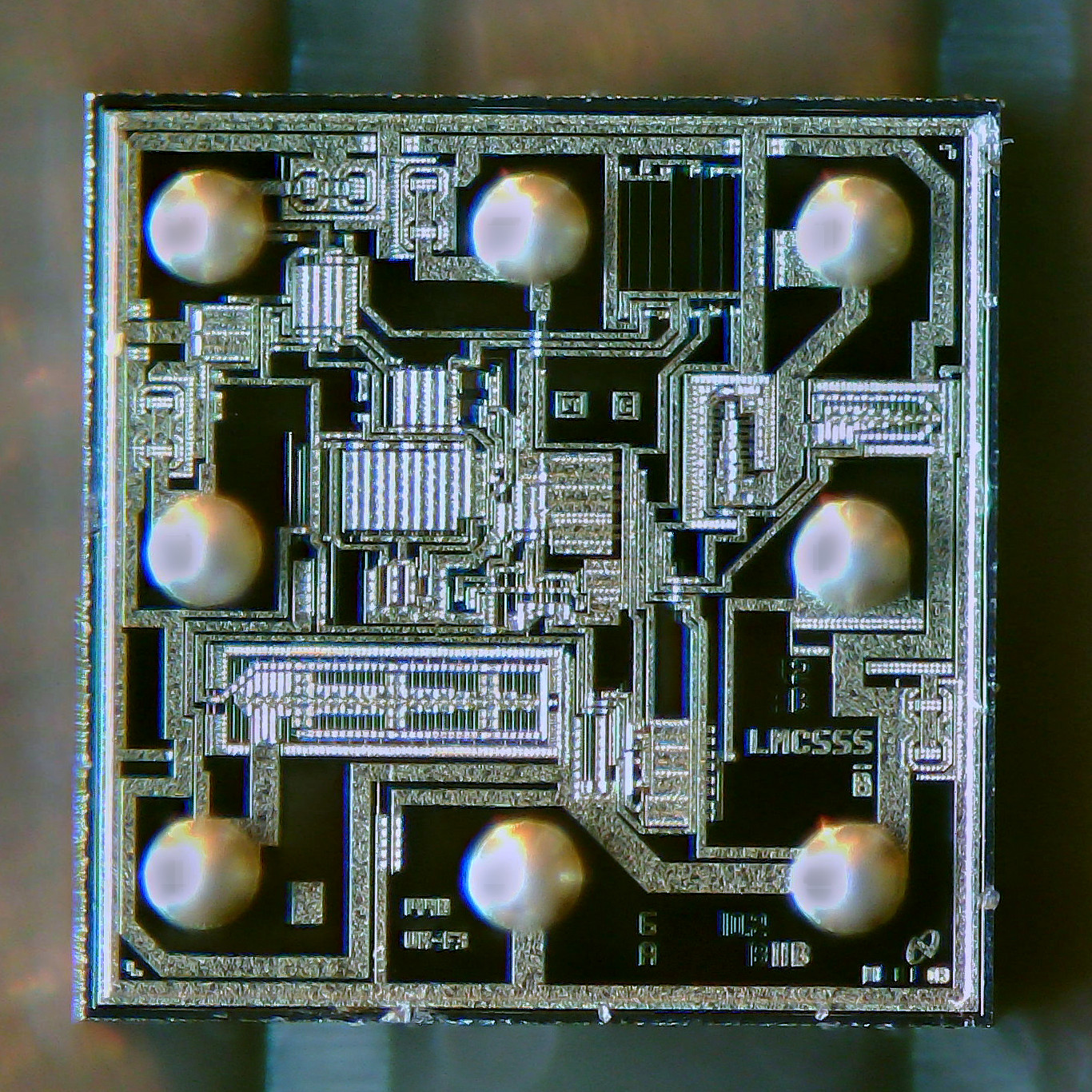
You may have heard the phrase “flip-chip” before: it’s a broad term referring to several integrated circuit packaging methods, the common thread being that the semiconductor die is flipped upside down so the active surface is closest to the PCB. As opposed to the more traditional method in which the IC is face-up and connected to the packaging with bond wires, this allows for ultimate packaging efficiency and impressive performance gains. We hear a lot about advances in the integrated circuits themselves, but the packages that carry them and the issues they solve — and sometimes create — get less exposure.
Let’s have a look at why semiconductor manufacturers decided to turn things on their head, and see how radioactive solder and ancient Roman shipwrecks fit in.
The Old Packages
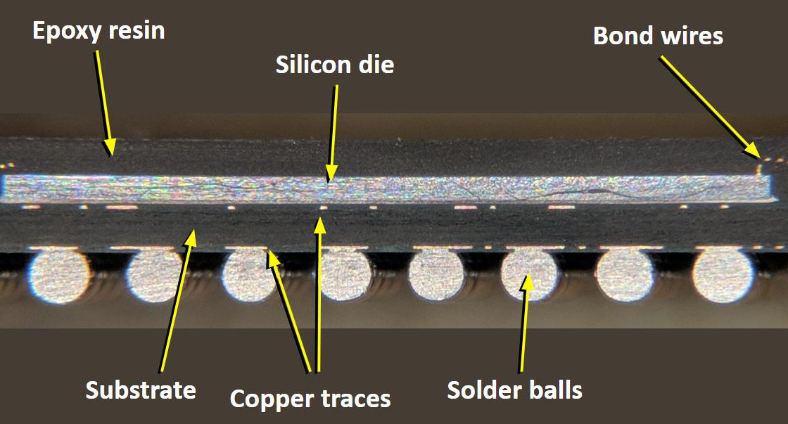
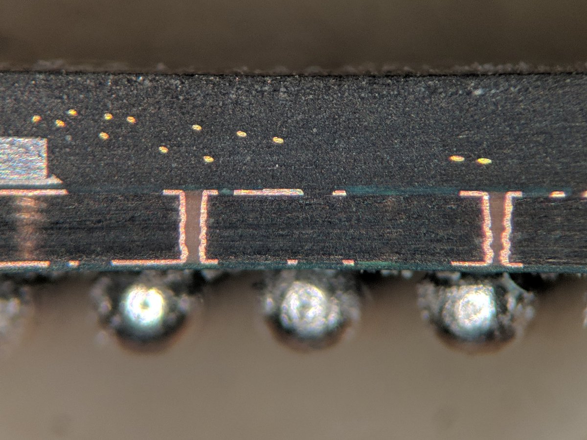
Very early integrated circuits were packaged in metal cans like the transistors of the day. Welded gold bond wires connected the die to the external pins. Open one of these old IC packages like a can of tuna, and the wires are plain to see. When DIP packages came about, they continued to use bond wires to connect the die to the IC pins, even though they were encapsulated in the plastic package.
This trend continued into surface-mount packages like SOIC, SSOP, and even BGAs, because it worked pretty well for parts from that period. But, as IC technology advanced, these packages became problematic. The first snag was the burgeoning size and complexity of the chips. As they grew, so did the number of connections required. Unfortunately, while the complexity grows with chip area, the number of possible wire-bond connections grows with the perimeter of both the die and the old-style packages. It’s X2 vs X, and at some point, there just isn’t enough space on the perimeter, so a more dense connection method had to be devised. A second problem was the performance of the wire bonds themselves. Like any conductor in free space, these little wires behave as inductors. This inductance can have serious consequences for high-speed circuits. As IC speeds increased, the inductance of the bond wires plus that of the package leads started to become a serious issue.
Flip Chips
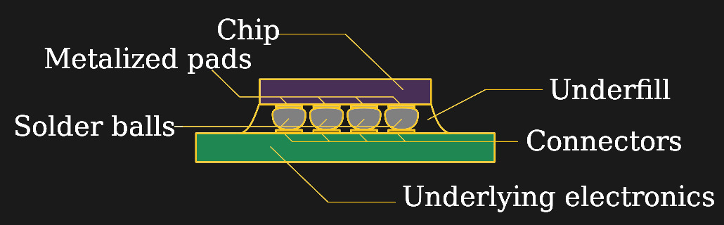
A good solution to both problems is to turn the semiconductor die upside down. With the chip flipped this way, the connections can be made directly from the chip to the next layer below without any bond wires. This allows for more connections, since bond pads can be placed anywhere; there’s no need to restrict them to the periphery of the die. For pad-limited designs with many I/O connections, this can actually result in a smaller chip. Additionally, the connections can be made with a short, thick metallic bump, which has much less inductance (around an order of magnitude less) than traditional bond wires.
In some cases, flip chips connect directly to printed circuit boards using solder balls. In others, the die may be connected first to traces on a substrate, similar to an intermediate PCB, that then connects to the board itself. Traces on this intermediate layer connect the solder bumps from the die to the board connections. This allows for fanning-out connections on the die that would otherwise be too closely pitched for PCB connections.
While we may think of flip-chip technology as the new kid on the block, it’s actually been around for a long time. IBM pioneered the idea for discrete diodes and transistors in their mainframe computers of the 1960s, and it was later adapted for use in automobile electronics in the 1970s. Today, the technique is commonplace, and used in a wide variety of applications.
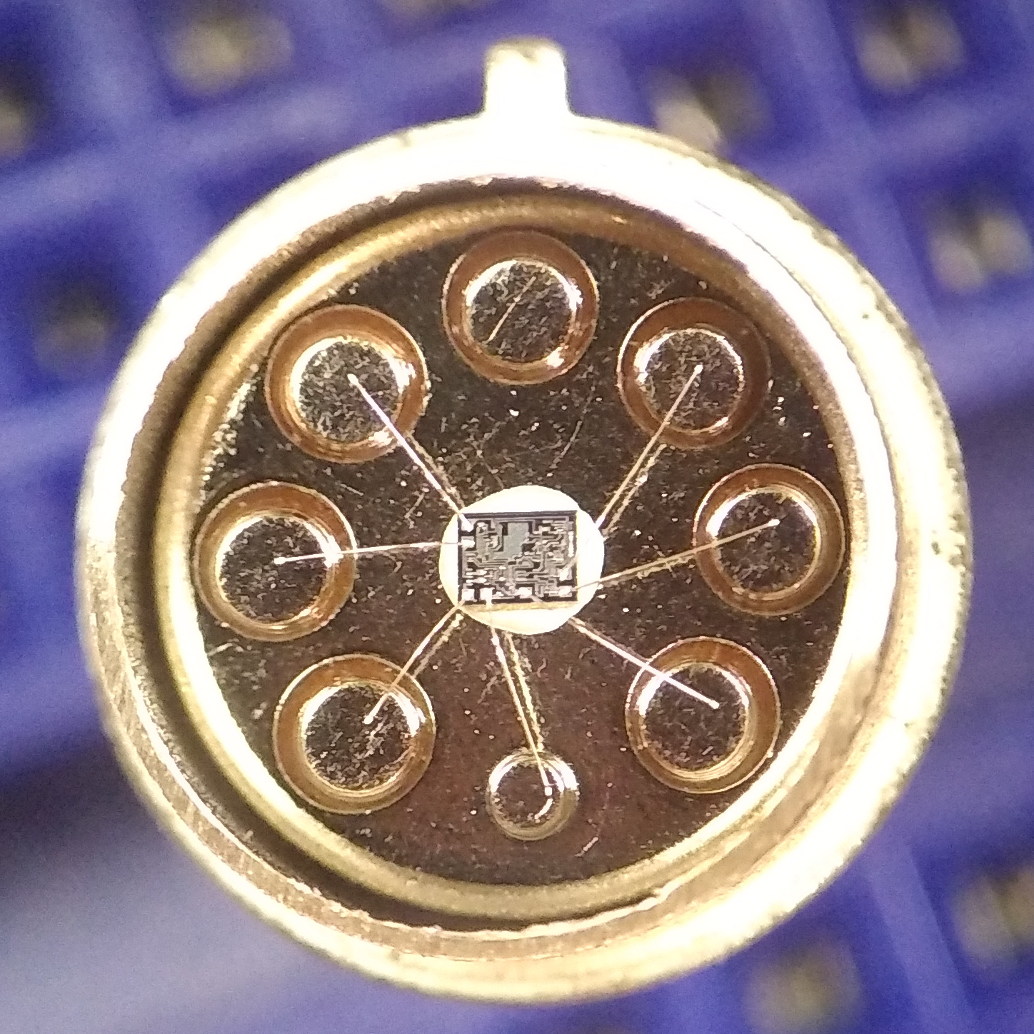
Not all leadless SMT packages have upside-down dice; there is a great diversity in IC packages. Some BGA packages use wire bonding, connecting the die pads to conductive traces on the package substrate before ultimately terminating in the solder balls on the bottom of the package. Likewise, the dice in QFN packages may be of either orientation. Sometimes the only way to know — just for curiosity’s sake — is to take a look inside the package.
Wafer-Level Chip-Scale Packaging
So, once you’ve decided to connect the die directly to the PCB, an interesting opportunity arises. You can turn the die into the packaging, and construct the whole assembly while the chips are still on the wafer. This is exactly what’s done in wafer-level chip-scale packaging (WLCSP). In this process, after the wafers have been manufactured, solder bumps are deposited on the bond pads, and an encapsulation coating is applied to both sides of the wafer. The now packaged chips, still on the wafer, are then tested and marked before being cut into individual units. This is a very efficient way to package the devices, and makes for a very efficient use of board space: since the package is the same size as the die, you just can’t get it any smaller.
While these chips are wonders of packaging efficiency, they can suffer some strange maladies. If you own a Raspberry Pi 2, you may be familiar with one of them. Shortly after its release, an interesting issue came to light when it was found that a bright flash (or a properly directed laser pointer) would interfere with the operation of a power regulator on the PCB, causing the Pi to reset. The chip in question was in a chip-size package with the die exposed below, and it turned out to be light-sensitive. Oops.
Maybe the most interesting problems with flip-chips, though, have to do with another sensitivity, specifically to alpha radiation.
Shipwrecks and Soft Errors
IBM first noticed in 1979 that their ceramic-DIP packaged DRAMs were susceptible to bit errors due to alpha particle emissions from the package lids. These alpha particles caused soft errors: one or more flipped bits with no damage to the hardware. Later, when flip chip packages became commonplace for complex ICs, soft error rates started to climb. The culprit: alpha particles emitted from tin-lead solder balls.
Alpha particles have very little penetrating power; a sheet of ordinary paper will stop them. Before flip chips, the packaging and even the silicon substrate itself provided adequate shielding, but when turned upside down, the sensitive side of the IC is now facing the solder. The resulting error rates could be alarmingly high. A Xilinx white paper from 2004, for instance, describes an issue arising from a packaging vendor incorrectly using high-alpha (i.e. “normal”) solder to assemble some of their flip-chip FPGAs, resulting in bit errors as often as every 230 hours of operation.
While we typically think of lead as a radiation shielding material, newly smelted lead is, in fact, slightly radioactive. Lead ore typically contains traces of uranium-238, which naturally decays (via a complicated chain) into a radioactive isotope of lead, Pb-210. Pb-210, in turn, eventually decays, with a half-life of 22 years, into Po-210, taking a brief stop as bismuth along the way. The final decay of Po-210 into stable Pb-206 releases an alpha particle, and that’s what causes the problems.
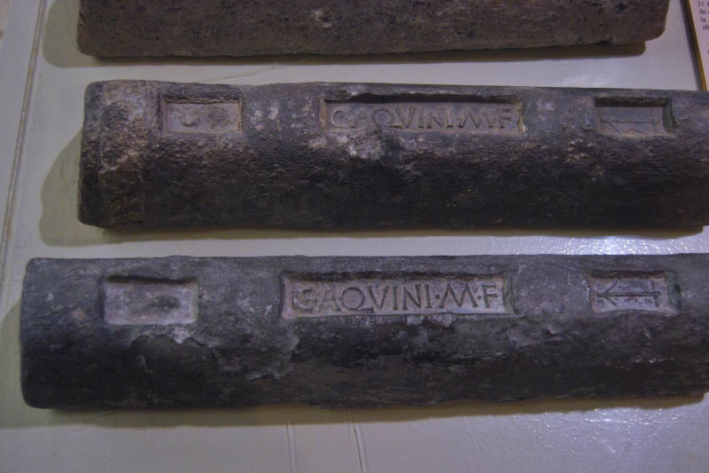
 Separating isotopes isn’t easy. This fact keeps nuclear weapons out of the hands of all but the few most powerful nation-states, but also makes it difficult to separate radioactive lead from the innocuous Pb-206. However, like most issues involving radioactivity, if you can wait long enough, the problem will go away by itself. Once the lead has been refined, the source of Pb-210 – the radio daughters of U-238 – is removed, and any existing radioactive isotopes begin to slowly cool off. After a few hundred years, very little alpha activity remains. So, one source for so-called low-alpha lead is metal that was refined in antiquity.
I remember around the turn of the century hearing about companies salvaging old lead from ancient shipwrecks to make low-alpha solder for vulnerable components, specifically the advanced microprocessors and FPGAs of the time. The lead was originally ballast or hull cladding, or carried as cargo, since it found use in an amazing variety of ways in ancient times – including plumbing for drinking water. Salvage companies would locate shipwrecks and other sources of ancient lead and scavenge it for use in sensitive electronic assemblies.
This practice would later become quite controversial as archaeologists grew concerned that valuable artifacts were being melted down, erasing cultural heritage. Although the headlines in 2013 were about physicists using ancient lead for neutrino experiments, by that time it was pretty clear that this isn’t a sustainable solution for electronic assembly. While some ore deposits are naturally less radioactive than others, and laser-based methods for isotope separation hold some promise, there aren’t really great solutions for economical low-alpha lead. For specialty applications where leaded solder is still required, alpha decay continues to be an expensive problem.
RoHS To The Rescue?
It would seem that with the RoHS directive, which mandates removal of the lead from solder, the alpha problem would be solved. Unfortunately, even at RoHS-allowed levels of contaminants, “lead-free” solders can still be hot enough to cause problems. In many cases, the activity of these so-called lead-free solders is due, surprisingly, to our old friend Pb-210. Lead is a natural contaminant in many metal ores, and tin sources may contain enough Pb-210 to cause problems for sensitive circuits, even when purified to “lead-free” solder standards. As a result, there’s an industry surrounding the production of low-alpha tin and RoHS-compliant solders, but of course, they aren’t cheap.
So, the next time you slap an IC onto a board, give a little thought to the package itself. And, if you’re seeing some strange behavior with your exposed-die part, consider your solder. You might just need some ancient lead.